| 4A B Building Zhuao Industrial Park Gushu Xixiang Baoan District Shenzhen,China,518126 | info@newbridge.com.cn |
| 4A B Building Zhuao Industrial Park Gushu Xixiang Baoan District Shenzhen,China,518126 | info@newbridge.com.cn |
 |
| Place of Origin: | SHENZHEN,CHINA |
| Brand Name: | NEWBRIDGE |
| Certification: | FCC,CE |
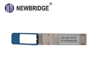
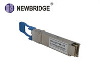
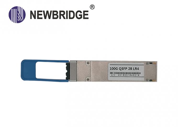
| Model Number: | ND-100GCFP- LR |
| Minimum Order Quantity: | 1PC |
|---|---|
| Price: | Negotiation |
| Packaging Details: | packing can be done by customer's requested, usually used in carton |
| Delivery Time: | According to the quantiy and stocking , 3-4 working days after payment |
| Payment Terms: | T/T , Western Union |
| Supply Ability: | According to the different products , the monthly output is different |
| Fiber: | Single Mode | Device Type: | Optical SFP Module |
|---|---|---|---|
| Data Rate: | 100G | Operating Temperature: | 0°C To 70°C |
| Distance: | 10km | Fiber Connector: | SC,FC,ST |
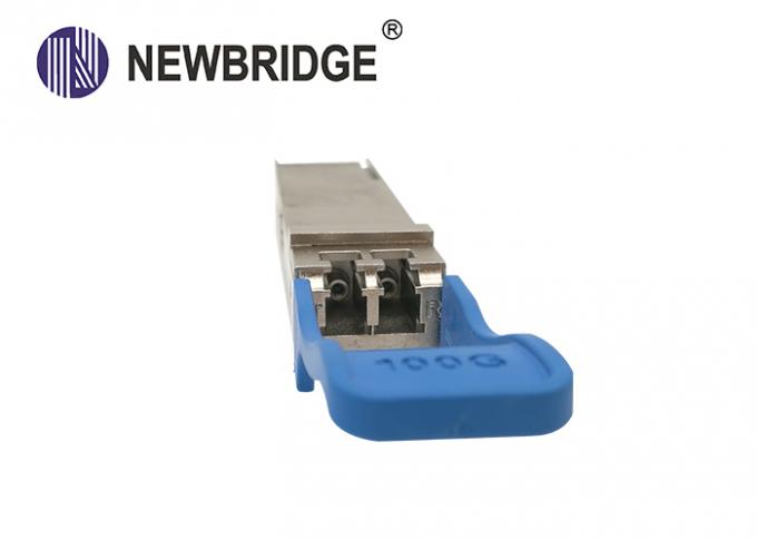
| Type: | QSFP28 Fiber Module |
Product Features
● Supports up to 112Gbps bit rates
● Duplex LC connector
● Hot pluggable
● Operating electrical serial data rate up to 27.952493Gbps
● 4 parallel electrical serial interface
● Applicable for 10km SMF connection
● Low power consumption, < 9W
● Digital Diagnostic Monitor Interfacel ●MDIO Communication Interface
● Compliant with 100GBASE-LR4 and OTU4
● Operating case temperature:
Commerical:-20 to 75 °C
Applications
● Local Area Network(LAN)
● Wide Area Network(WAN)
● Switch to router interface
● ITU-T OTU4 OTL4.4
Standards
● Compliant with IEEE 802.3ba
● Compliant with CFP2 MSA hardware specifications
● Compliant with CFP2 MSA management specifications
● Compliant with ITU-T G709/Y.1331
● Compliant with RoHS
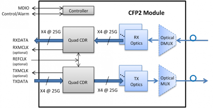
Functional Description
The 100G CFP2 LR4 optical transceiver integrates the transmit and receive path onto one module. On the transmit side, four lanes of serial data streams are recovered, retimed,and passed on to four laser drivers, which control four electric-absorption modulated lasers (EMLs) with 1296, 1300, 1305, and 1309 nm center wavelengths. The optical signals are then multiplexed into a single-mode fiber through an industry-standard LC connector.On the receive side, 4 lanes of optical data streams are optically demultiplexed by an integrated optical demultiplexer. Each data steam is recovered by a PIN photodetector and transimpedance amplifier, retimed, and passed on to an output driver. This module features a hot-pluggable electrical interface, low power consumption, and MDIO management interface.
Functional Diagram
Absolute Maximum Ratings
| Parameter | Symbol | Min. | Max. | Unit | Note |
| Supply Voltage | Vcc | -0.5 | 3.6 | V | |
| Storage Temperature | TS | -40 | 85 | °C | |
| Relative Humidity | RH | 0 | 85 | % |
Note: Stress in excess of the maximum absolute ratings can cause permanent damage to the transceiver.
Recommended Operating Conditions
| Parameter | Symbol | Min. | Typ | Max. | Unit | Note |
| Data Rate | DR | 103.2 | 11.3 | Gb/s | ||
| Supply Voltage | Vcc | 3.14 | 3.3 | 3.46 | V | |
| Operating Case Temp. | Tc | 0 | 70 | °C |
Electrical Characteristics
(Tested under recommended operating conditions,unless otherwise noted)
| Parameter | Symbol | Unit | Min | Typ | Max | Notes | ||||
| Voltage Supply Electrical Characteristics | ||||||||||
| Supply Current | Tx Section | Icc | A | 3.75 | 1 | |||||
| Rx Section | ||||||||||
| Power Supply Noise | Vrip | 2% DC | 1MHz | |||||||
| 3% 1 | 10MHz | |||||||||
|
Total Dissipation Power |
Class1 | Pw | W | 3 | ||||||
| Class2 | 6 | |||||||||
| Class3 | 9 | |||||||||
| Class4 | 12 | |||||||||
| Low Power Mode Dissipation | Plow | W | 2 | |||||||
| Inrush Current | Class1 |
and |
I-inrush | mA/usec | 100 | |||||
| Turn-off Current | Class2 | I-turnoff | mA/usec | -100 | ||||||
| Inrush Current | Class3 |
and
|
I-inrush | mA/usec | 200 | |||||
| Turn-off Current | Class4 | I-turnoff | mA/usec | -200 | ||||||
| Different Signal Electrical Characteristics | ||||||||||
| Single Ended Data Input Swing | mV | 20 | 525 | |||||||
| Single Ended Data Output Swing | mV | 180 | 385 | |||||||
| Differential Signal Output Resistance | Ω | 80 | 120 | |||||||
| Differential Signal Input Resistance | Ω | 80 | 120 | |||||||
| 3.3V LVCMOS Electrical Characteristics | ||||||||||
| Input High Voltage | 3.3VIH | V | 2.0 | Vcc+0.3 | ||||||
| Input Low Voltage | 3.3VIL | V | -0.3 | 0.8 | ||||||
| Input Leakage Current | 3.3IIN | uA | -10 | +10 | ||||||
| Output HighVoltage (IOH=100uA) | 3.3VOH | V | Vcc-0.2 | |||||||
| Output Low Voltage (IOL=100uA) | 3.3VOL | V | 0.2 | |||||||
|
Minimum Pulse Width of Control Pin Signal |
t_CNTL | us | 100 | |||||||
| 1.2V LVCMOS Electrical Characteristics | ||||||||||
| Input High Voltage | 1.2VIH | V | 0.84 | 1.5 | ||||||
| Input Low Voltage | 1.2VIL V | 0.3 | 1.2VIL V | 0.36 | ||||||
| Input Leakage Current | 1.2IIN | uA | -100 | +100 | ||||||
| Output High Voltage | 1.2VOH | V | 1.0 | 1.5 | ||||||
| Output Low Voltage | 1.2VOL | V | -0.3 | 0.2 | ||||||
| Output High Current | 1.2IOH | mA | -4 | |||||||
| Output Low Current | 1.2IOL | mA | +4 | |||||||
| Input Capacitance | Ci | pF | 10 | |||||||
High Speed Electrical Characteristics
| Parameter | Symbol | Unit | Min. | Max. | Notes |
| Impedance | Zd | Ω | 90 | 110 | |
| Frequency | MHz | 161.1328125 | 1/64 of electrical lane rate | ||
| Frequency Stability | △f | ppm | -100 | 100 | For Ethernet |
| -20 | 20 | For Telecom | |||
| Differential Voltage | VDIFF | mV | 400 | 900 | Peak to Peak Differential |
| Common mode noise (rms) | mV | 17.5 | |||
| RMS jitter | ps | 10 | Random Jitter Over frequency band of 10KHZ<f<10MHZ | ||
| Clock Duty Cycle | % | 40 | 60 | ||
Optical Characteristics
(Tested under recommended operating conditions,unless otherwise noted)
| Parameter | Symbol | Unit | Min | Typ | Max | Notes | |||||
| Optical Transmitter Characteristics | |||||||||||
| Signaling rate, each lane | GBd | 25.78125 ±100 ppm | 100GBase-LR4 | ||||||||
| 27.9525 ±20 ppm | OTU4 | ||||||||||
| Four Lane Wavelength Range | λ1 | nm | 1294.53 | 1295.56 | 1296.59 | ||||||
| λ2 | 1299.02 | 1300.05 | 1301.09 | ||||||||
| λ3 | 1303.54 | 1304.58 | 1305.63 | ||||||||
| λ4 | 1308.09 | 1309.14 | 1310.19 | ||||||||
| Total launch power | dBm | 10.5 | 100GBase-LR4 | ||||||||
| 10 | OTU4 | ||||||||||
| Average launch power, each lane | Pavg | dBm | -4.3 | 4.5 | 2 | ||||||
| -0.6 | 4 | ||||||||||
| Optical modulation amplitude, each lane (OMA)2 | OMA | dBm | -1.3 | 4.5 | |||||||
| Difference in launch power between any two lanes (OMA) | dB | 5 | |||||||||
| Extinction ratio | ER | dB | 4 | 100GBase-LR4 | |||||||
| 4 | 6.5 | OTU4 | |||||||||
| Side-mode suppression ratio | SMSR | dB | 30 | ||||||||
| Transmitter and dispersion penalty, each lane | TDP | dB | 2.2 | ||||||||
| Optical return loss tolerance | dB | 20 | |||||||||
| Transmitter reflectance3 | dB | –12 | |||||||||
| Transmitter eye mask {X1, X2, X3, Y1, Y2, Y3} | {0.25, 0.4, 0.45, 0.25, 0.28, 0.4} | 100GBase-LR4 | |||||||||
| Optical Receiver Characteristics | |||||||||||
| Receive Rate for Each Lane | Gbps | 25.78125 | 27.9525 | ||||||||
| Overload Input Optical Power | Pmax | dBm | 5.5 | 3 | |||||||
|
Average Receive Power for Each Lane |
Pin | dBm | -8.6 + ∆ | 3 | 4, 5 | ||||||
|
Receive Power In OMA for Each Lane |
PinOMA | dBm | 3 | ||||||||
|
Difference in Receive Power in OMA between Any Two Lanes |
dBm | ||||||||||
|
Receiver Sensitivity in OMA for Each Lane |
SOMA | dBm | -8.6 | 6 | |||||||
|
Stressed Receiver Sensitivity in OMA for Each Lane |
dBm | -6.8 | 7, 8 | ||||||||
Notes:
1. The supply current includes CFP2 module’s supply current and test board workingcurrent.
2. Average launch power, each lane (min) is informative for 100GBase-LR4, not the principal indicator of signal strength.
3.The receiver shall be able to tolerate , without damage, continuous exposure to an optical input signal having this average power level
4. The average receive power , each lane (max) for 100GBASE-ER4 is larger than the
100BASE-ER4 transmitter value to allow compatibility with 100BASE-LR4 units at short distances
5. Average receive power, each lane (min) is informative and not the principal indicator
of signal strength. A received power below this value cannot be compliant; however, a value above this does not ensure compliance
6. Receiver sensitivity (OMA), each lane (max) is informative
7. Measured with conformance test signal at TP3 for BER=10-12
8. conditions of stressed receiver sensitivity test: vertical eye closure penalty for each lane is 1.8dB;stressed eye J2 jitter for each lane is 0.3UI; stressed eye J9 jitter for each lane is 0.47UI.
| Pin | Name | I/O | Logic | Description |
| 1 | GND | |||
| 2 | (TX_MCLKn) | O | CML | For optical waveform testing. Not for normal use. |
| 3 | (TX_MCLKp) | O | CML | For optical waveform testing. Not for normal use. |
| 4 | GND | |||
| 5 | N.C | No Connect | ||
| 6 | N.C | |||
| 7 | 3.3V_GND | 3.3V Module Supply Voltage Return Ground, can be separate or tied together with Signal Ground | ||
| 8 | 3.3V_GND | |||
| 9 | 3.3V | 3.3V Module Supply Voltage | ||
| 10 | 3.3V | |||
| 11 | 3.3V | |||
| 12 | 3.3V | |||
| 13 | 3.3V_GND | 3.3V Module Supply Voltage Return Ground, can be separate or tied together with Signal Ground | ||
| 14 | 3.3V_GND | |||
| 15 | VND_IO_A | I/O | Module Vendor I/O A. Do Not Connect! | |
| 16 | VND_IO_B | I/O | Module Vendor I/O A. Do Not Connect! | |
| 17 | PRG_CNTL1 | I | LVCMOS w/ PUR | Programmable Control 1 set over MDIO, MSA Default: TRXIC_RSTn, TX & RX ICs reset, "0": reset, "1" or NC: enabled = not used |
| 18 | PRG_CNTL2 | I | LVCMOS w/ PUR | Programmable Control 2 set over MDIO, MSA Default: Hardware Interlock LSB, "00": ≤3W, "01": ≤6W, "10": ≤9W, "11" or NC: ≤12W = not used |
| 19 | PRG_CNTL3 | I | LVCMOS w/ PUR | Programmable Control 2 set over MDIO, MSA Default: Hardware Interlock LSB, "00": ≤3W, "01": ≤6W, "10": ≤9W, "11" or NC: ≤12W = not used |
| 20 | PRG_ALRM1 | O | LVCMOS | Programmable Alarm 1 set over MDIO, MSA Default: HIPWR_ON, "1": module power up completed, "0": module not high powered up |
| 21 | PRG_ALRM2 | O | LVCMOS | Programmable Alarm 2 set over MDIO, MSA Default: MOD_READY, "1": Ready, "0": not Ready. |
| 22 | PRG_ALRM3 | O | LVCMOS | Programmable Alarm 3 set over MDIO, MSA Default: MOD_FAULT, fault detected, "1": Fault, "0": No Fault |
| 23 | GND | |||
| 24 | TX_DIS | I | LVCMOS w/ PUR | Transmitter Disable for all lanes, "1" or NC = transmitter disabled, "0" = transmitter enabled |
| 25 | RX_LOS | O | LVCMOS | Receiver Loss of Optical Signal, "1": low optical signal, "0": normal condition |
| 26 | MOD_LOPWR | I | LVCMOS w/ PUR | Module Low Power Mode. "1" or NC: module in low power (safe) mode, "0": power-on enabled |
| 27 | MOD_ABS | O | GND | Module Absent. "1" or NC: module absent, "0": module present, Pull Up Resistor on Host |
| 28 | MOD_RSTn | I | LVCMOS w/ PDR | Module Reset. "0" resets the module, "1" or NC = module enabled, Pull Down Resistor in Module |
| 29 | GLB_ALRMn | O | LVCMOS | Global Alarm. “0": alarm condition in any MDIO Alarm register, "1": no alarm condition, Open Drain, Pull Up Resistor on Host |
| 30 | GND | |||
| 31 | MDC | I | 1.2VCMOS | Management Data Clock (electrical specs as per IEEE Std 802.3ae-2008 and ba-2010) |
| 32 | MDIO | I/O | 1.2VCMOS | Management Data I/O bi-directional data (electrical specs as per IEEE Std 802.3ae-2008 and ba-2010) |
| 33 | PRTADR0 | I | 1.2VCMOS | MDIO Physical Port address bit 0 |
| 34 | PRTADR1 | I | 1.2VCMOS | MDIO Physical Port address bit 1 |
| 35 | PRTADR2 | I | 1.2VCMOS | MDIO Physical Port address bit 2 |
| 36 | VND_IO_C | I/O | Module Vendor I/O C. Do Not Connect! | |
| 37 | VND_IO_D | I/O | Module Vendor I/O D. Do Not Connect! | |
| 38 | VND_IO_E | I/O | Module Vendor I/O E. Do Not Connect! | |
| 39 | 3.3V_GND | |||
| 40 | 3.3V_GND | |||
| 41 | 3.3V | 3.3V Module Supply Voltage | ||
| 42 | 3.3V | |||
| 43 | 3.3V | |||
| 44 | 3.3V | |||
| 45 | 3.3V_GND | |||
| 46 | 3.3V_GND | |||
| 47 |
N.C
|
No Connect
|
||
| 48 |
N.C
|
|||
| 49 |
GND
|
|||
| 50 |
(RX_MCLKn)
|
O | CML | For optical waveform testing. Not for normal use. |
| 51 |
(RX_MCLKp)
|
O | CML | |
| 52 | GND | |||
| 53 | GND | |||
| 54 | N.C. | |||
| 55 | N.C. | |||
| 56 | GND | |||
| 57 | RX0p | 25 Gbps receiver data; Lane 0 | ||
| 58 | RX0n | 25 Gbps receiver data bar; Lane 0 | ||
| 59 | GND | |||
| 60 | RX1p | 25 Gbps receiver data; Lane 1 | ||
| 61 | RX1n | 25 Gbps receiver data bar; Lane 1 | ||
| 62 | GND | |||
| 63 | N.C. | |||
| 64 | N.C. | |||
| 65 | GND | |||
| 66 | N.C. | |||
| 67 | N.C. | |||
| 68 | GND | |||
| 69 | RX2p | 25 Gbps receiver data; Lane 2 | ||
| 70 | RX2n | 25 Gbps receiver data bar; Lane 2 | ||
| 71 | GND | |||
| 72 | RX3p | 25 Gbps receiver data; Lane 3 | ||
| 73 | RX3n | 25 Gbps receiver data bar; Lane 3 | ||
| 74 | GND | |||
| 75 | N.C. | |||
| 76 | N.C. | |||
| 77 | GND | |||
| 78 | (REFCLKp) | CML | Module reference clock. No connect. | |
| 79 | (REFCLKn) | CML | Module reference clock. No connect. | |
| 80 | GND | |||
| 81 | N.C. | |||
| 82 | N.C. | |||
| 83 | GND | |||
| 84 | TX0p | 25 Gbps transmitter data; Lane 0 | ||
| 85 | TX0n | 25 Gbps transmitter data bar; Lane 0 | ||
| 86 | GND | |||
| 87 | TX1p | 25 Gbps transmitter data; Lane 1 | ||
| 88 | TX1n | 25 Gbps transmitter data bar; Lane 1 | ||
| 89 | GND | |||
| 90 | N.C. | |||
| 91 | N.C. | |||
| 92 | GND | |||
| 93 | N.C. | |||
| 94 | N.C. | |||
| 95 | GND | |||
| 96 | TX2p | 25 Gbps transmitter data; Lane 2 | ||
| 97 | TX2n | 25 Gbps transmitter data bar; Lane 2 | ||
| 98 | GND | |||
| 99 | TX3p | 25 Gbps transmitter data; Lane 3 | ||
| 100 | TX3n | 25 Gbps transmitter data bar; Lane 3 | ||
| 101 | GND | |||
| 102 | N.C. | |||
| 103 | N.C. | |||
| 104 | GND |
Hardware Control Pins
The CFP2 Module support real-time control functions via hardware pins, listed in the following
| Pin | Symbol | Description | I/O | Logic | H | L | Pull-up/down |
| 17 | PRG_CNTL1 |
Programmable Control 1 MSADefault:TRXIC_RST n , TX&RX ICs reset, “0”:reset;”1” |
I |
3.3V LVCMOS |
per CFP MSA Management Interface Specification |
Pull-Up Note1 |
|
|
18
|
PRG_CNTL2 |
Programmable Control 2 MSADefault :Hardware Interlock LSB |
I
|
3.3V LVCMOS |
Pull-Up Note1 |
||
| 19 | PRG_CNTL3 |
Programmable Control 3 MSA Default:Hardware Interlock MSB |
I |
3.3V LVCMOS |
Pull-Up Note1 |
||
| 26 | MOD_LOPWR | Module Low Power Mode | I |
3.3V LVCMOS Low Power Enable Pull-Up |
Low Power |
Enable |
Pull-Up Note1 |
| 28 | MOD_RSTn | Module Reset(Invert) | I |
3.3V LVCMOS |
Enable | Reset |
Pull-Down Note2 |
Notes:
1. Pull-Up resistor (4.7KOhm to 10 KOhm) is located within the CFP2 module
2. Pull-Down resistor (4.7KOhm to 10 kOhm) is located within the CFP2 module
Hardware Alarm Pins
The CFP2 Module supports alarm hardware pins listed in the following
| Pin | Symbol | Description | I/O | Logic | H | L | Pull-up/down | |
| 20 |
PRG_ALRM 1 |
Programmable Alarm 1 MSA Default:HIPWR_ON |
O | 3.3V LVCMOS |
Active High per MDIO document |
|
||
| 21 | PRG_ALRM2 |
Programmable Alarm 2 MSA default:MOD_READY , Ready State has been reached |
O | 3.3V LVCMOS | ||||
| 22 |
PRG_ALRM 3 |
Programmable Alarm 3 MSA Default: MOD_FAULT |
O | 3.3V LVCMOS | ||||
| 27 | MOD_ABS | Module Absent | O | 3.3V LVCMOS | Absent | Present |
Pull-Down Note1 |
|
| 25 | RX_LOS |
Receiver Loss of Signa |
O | 3.3V LVCMOS |
Loss of Signal |
OK | ||
Note:
1:.Pull-Down resistor (<100Ohm) is located within the CFP2 module. Pull-up should be located on the host
Management Interface Pins(MDIO)
The CFP2 Module supports alarm, control and monitor functions via an MDIO bus. The CFP2 MDIO pins are listed in the following:
| . | Symbol | Description | I/O | Logic | H | L | Pull-up/down |
| 29 | GLB-ALRMn | Global Alarm | I |
3.3V LVCMOS |
OK | Alarm | |
| 32 | MDIO |
Management interface bidirectional data |
I/O | 1.2V LVCMOS | |||
| 31 | MDC | Management interface clock input | I | 1.2V LVCMOS | |||
| 33 | PRTADR0 | MDIO physical port address bit 0 | I | 1.2V LVCMOS | Per MDIO | ||
| 34 | PRTADR1 | MDIO physical port address bit 1 | I | 1.2V LVCMOS | |||
| 35 | PRTADR2 | MDIO physical port address bit 2 | I | 1.2V LVCMOS | |||
Hardware Signaling Pin Timing Requirements
Timing Parameters for CFP2 hardware Signal Pins are listed in the following:
| Parameter | Symbol | Unit | Min. | Max. | Notes |
| Hardware MOD_LOPWR assert | t_MOD_LOPWR_assert | ms | 1 | ||
| Hardware MOD_LOPWR deassert | t_MOD_LOPWR_deassert | s | 60 | Stored in NVR register 8072h | |
| Management interface clock period | t_prd | ns | 250 | MDC is 4 MHz rate or less | |
| Host MDIO setup time | t_setup | ns | 10 | ||
| Host MDIO hold time | t_hold | ns | 10 | ||
| CFP2 MDIO delay time | t_delay | ns | 0 | 175 | |
| GLB_ALRM assert time | GLB_ALRMn_assert | ms | 150 |
A logic “OR” of associated MDIO alarm and status registers |
|
| GLB_ALRM deassert time | GLB_ALRMn_deassert | ms | 150 |
A logic “OR” of associated MDIO alarm and status registers |
|
| Minimum pulse width of control pin signal | t_CNTL | μs | 100 | ||
| Initialization time from reset | t_initialize | s | 2.5 | ||
| TX_Disable assert time | t_deassert | μs | 100 | Transmitter disable, application specific | |
| TX_Disable deassert time1 | t_assert | ms | 5 |
Time from Tx Disable pin deasserted until CFP2 module enters the Tx-turn-on state Stored in NVR register 8073h |
|
| RX_LOS assert time | t_loss_assert | μs | 100 |
From occurrence of loss of signal to assertion of RX_LOS |
|
| RX_LOS deassert time | t_loss_deassert | μs | 100 |
From occurrence of return of signal to deassert of RX_LOS |
CFP2 Lane Assignment
| Lane | Center Frequency | Center Wavelength | Wavelength Range |
| L0 | 231.4 THz | 1295.56 nm | 1294.53 to 1296.59 nm |
| L1 | 230.6 THz | 1300.05 nm | 1299.02 to 1301.09 nm |
| L2 | 229.8 THz | 1304.58 nm | 1303.54 to 1305.63 nm |
| L3 | 229.0 THz | 1309.14 nm | 1308.09 to 1310.19 nm |
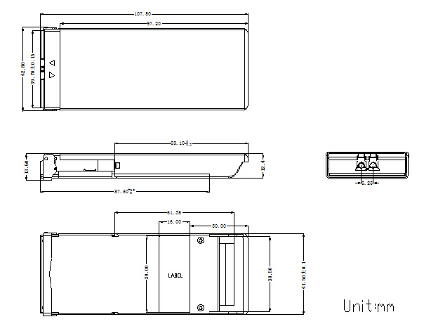
Package Dimensions
Ordering Information
| Part Number | Description |
| ND-100GCFP-LR | 100G CFP2 LR4 10Km -20~75℃ |


SD HD SDI Converter , 20km 40km 60km Optional Mini Converter with single mode or single fiber
DC 12V Hdmi To Hd Sdi Converter SDI Signal Loop Out With 158×120×36mm Size
5V~24VDC Hdmi To Hd Sdi Converter 720p/1080p With 2 Channel SDI Signal Out
Plug And Play 60km HD SDI Converter , SD Auto Detection Optical Transceiver
RJ45 Port 100M Industrial Ethernet Switch/8 PoE port industrial network switch
High Efficiency 8 Port SFP PoE Ethernet Switch High Efficiency Easy Operating
Full Duplex Operation 24 Port PoE Ethernet Switch RJ45 Ports 100m 8.8G
LCD Display 16 Port Ethernet Switch 10 100Mbps 2G TP / SFP AC 240V Accurate
3D Video 4K HD HDMI Splitter 1 x 8 HDMI Splitter 1 In 8 Out
4K 1.4b 1 x 4 HDMI Splitter 1 In 4 Out Supporting 3D Video CE Certification
100Mbps RJ45 DC output 12V port poe splitter support IEEE 802.3at Poe Splitter HD HDMI Splitter